F4BM300 High Frequency PCB - 2-Layer Rigid PCB with Immersion Tin Finish
1. Introduction of F4BM300
Wangling's F4BM300 laminates are expertly crafted through a precise formulation and rigorous pressing of fiberglass cloth, polytetrafluoroethylene (PTFE) resin, and PTFE film. This laminate offers enhanced electrical performance compared to the F4B300, featuring reduced dielectric loss, increased insulation resistance, and improved stability. It serves as a viable alternative to similar foreign products.
F4BM300 and F4BME300 share the same dielectric layer; however, they differ in their copper foil configurations. F4BM300 utilizes ED copper foil, making it ideal for applications that do not require Passive Intermodulation (PIM) performance. In contrast, F4BME300 is paired with reverse-treated foil (RTF) copper foil, which delivers superior PIM performance, greater precision in line control, and reduced conductor loss.
By adjusting the ratio of PTFE to fiberglass cloth, both F4BM300 and F4BME300 achieve precise control over the dielectric constant, resulting in low loss and enhanced dimensional stability. A higher dielectric constant is associated with a greater proportion of fiberglass, yielding improved dimensional stability, a lower thermal expansion coefficient, enhanced temperature drift, and a slight increase in dielectric loss.
2. Features of F4BM300
Dielectric constant (Dk) of 3.0 at 10 GHz
Dissipation factor of 0.0017 at 10 GHz
Coefficient of Thermal Expansion (CTE) of 12 ppm/°C in the x-axis, 15 ppm/°C in the y-axis, and 95 ppm/°C in the z-axis, operating from -55°C to 288°C
Low thermal coefficient of Dk at -80 ppm/°C within the range of -55°C to 150°C
Moisture absorption of ≤0.08%
Flammability rating of UL-94 V0
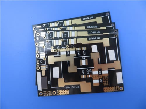
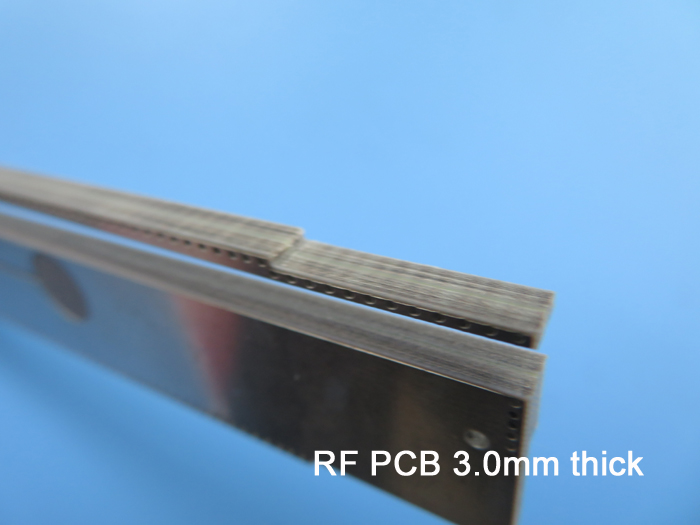
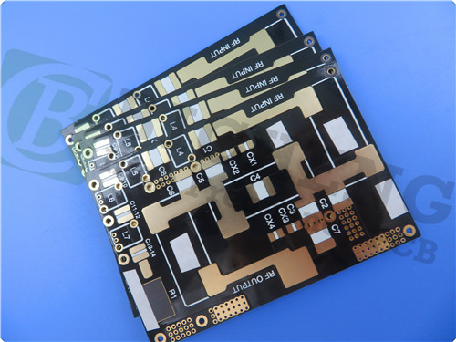
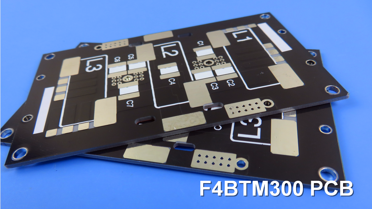
3. PCB Stackup: 2-Layer Rigid PCB
The stackup includes a copper layer of 35 µm, followed by a 1.524 mm core of F4BM300, and another copper layer of 35 µm.
4. PCB Construction Details
Board dimensions measure 700 mm x 40 mm for one piece, with a tolerance of ±0.15 mm.
The minimum trace and space specifications are 5/5 mils.
The minimum hole size is 0.4 mm.
There are no blind vias.
The finished board thickness is 1.6 mm.
The final copper weight for the outer layers is 1 oz (1.4 mils).
Via plating thickness is 20 µm.
The surface finish is immersion tin.
The top silkscreen is white, while the bottom silkscreen is not included.
The top and bottom solder masks are both green.
A 100% electrical test is conducted prior to shipment.
5. PCB Statistics
Total components: 51
- Total pads: 76
Through-hole pads: 37
Top SMT pads: 49
Bottom SMT pads: 0
Vias: 32
Nets: 2
6. Type of Artwork Supplied
The artwork is provided in Gerber RS-274-X format.
7. Quality Standard
The product complies with IPC-Class-2 standards.
8. Availability
F4BM300 is available globally.
9. Typical Applications
Microwave, RF, and radar systems
Phase shifters
Power dividers, couplers, and combiners
Feed networks
Phase-sensitive antennas and phased array antennas
Satellite communications
Base station antennas
|

.jpg)